|
|
The SignalTap® II Logic Analyzer lets you capture signal activity from internal PLD nodes while the system under test is running at speed. Samples are saved to internal memory resources when the logic analyzer is triggered and streamed off chip via the JTAG port. Optional trigger input, trigger output, and debug port signals can be routed to spare I/O pins to synchronize the logic analyzer with external equipment and vice-versa.
The SignalTap II window has two views: the Setup tab and the Data tab. In the Setup tab, you can add nodes to a SignalTap II File (.stp) and configure analyzer settings. In the Data tab, you can view captured logic events as waveforms.
You can create multiple instances in an STP File. Each instance contains an Embedded Logic Analyzer megafunction. You can configure settings for each instance, such as the clock source, sample depth, data and trigger input width, trigger levels, and trigger input and output.
You can compile the STP File with the rest of your design and download it to the target device. You can then run the SignalTap II Logic Analyzer. If you want, you can run multiple instances simultaneously.
After a full compilation with the current configuration, including the number of data nodes and trigger nodes manually allocated and SignalTap II pre-synthesis and post-fitting nodes, you can perform SignalTap II incremental routing to speed up the debug process. You can perform incremental routing by adding and removing SignalTap II post-fitting nodes, and removing SignalTap II pre-synthesis node that you allocated for incremental routing in the initial full compilation, as long as the number of data or trigger nodes in the current instance does not exceed the number of manually specified data or trigger nodes allocated.
The SignalTap II Logic Analyzer captures data, offloads it from the target device, and displays it as a waveform in an STP File. You can edit the bus value of a SignalTap II waveform by specifying a data format, or using a mnemonic table. You can also insert time bars in the waveforms, print waveform data, export waveform data, and generate a text file containing a list of the captured data.
Each instance in a SignalTap II File (.stp) contains an Embedded Logic Analyzer megafunction. When acquiring data, the Embedded Logic Analyzer megafunction requires internal device resources, such as logic elements, embedded system blocks (ESB) or M4K memory blocks, and I/O pins.
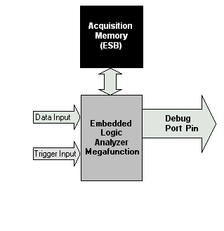
The SignalTap II Logic Analyzer saves acquired data to internal memory.
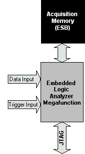
The advantages of internal RAM are that it does not use I/O pins or require external test equipment. However, it uses ESBs, and its sample depth is limited to available ESBs.
Debug port signals can be routed to spare I/O pins for capture by an external logic analyzer or oscilloscope. One I/O pin is used for each signal.
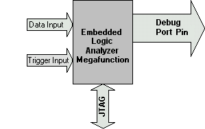
The advantages of debug port pins are that they do not use ESBs and their sample depth is limited only by external test equipment. However, they use I/O pins, and require external test equipment to capture signals.
The number of logic elements used by the Embedded Logic Analyzer megafunction is based on data/trigger input width, sample depth, trigger levels, and the number of instances in the STP File. You can select up to 1024 nodes in each instance.
The following table shows the approximate number of logic elements needed for various signal "widths" with APEX™ 20K, APEX™ II, ARM®-based Excalibur™, Cyclone™, Mercury™, Stratix™, or Stratix™ GX devices:
| Signals | Logic Elements |
|---|---|
| 1 | 167 |
| 2 | 180 |
| 4 | 202 |
| 8 | 246 |
| 16 | 327 |
| 32 | 495 |
| 64 | 823 |
| 128 | 1484 |
The number of ESBs or M4K memory blocks used by the Embedded Logic Analyzer megafunction is a function of the number of input signals assigned (width), and the number of samples saved (depth). The table below shows the number of ESBs or M4K memory blocks needed for various sample buffer depths and input signal widths:
| Samples (Depth) | |||||||
|---|---|---|---|---|---|---|---|
| 0 | 128 | 256 | 512 | 1024 | 2048 | ||
| Signals (Width) | 1 | 0 | 1 | ||||
| 2 | 0 | 1 | 2 | ||||
| 4 | 0 | 1 | 2 | 4 | |||
| 8 | 0 | 1 | 2 | 4 | 8 | ||
| 16 | 0 | 1 | 2 | 4 | 8 | 16 | |
| 32 | 0 | 2 | 4 | 8 | 16 | 32 | |
| 64 | 0 | 4 | 8 | 16 | 32 | 64 | |
| 128 | 0 | 8 | 16 | 32 | 64 | 128 | |
You can configure the SignalTap II Logic Analyzer using a combination of these resources to fit your application.
|
| More information is available on the SignalTap II Logic Analyzer on the Altera® web site. | |
|
- PLDWorld - |
|
|
| Created by chm2web html help conversion utility. |